

The Chip Is Cheap. Silicon Photonics Alignment Is Not.
Lining up a hair-thin fibre with a photonic chip eats most of the manufacturing budget — and the industry's answer is to stop doing it one step at a time.

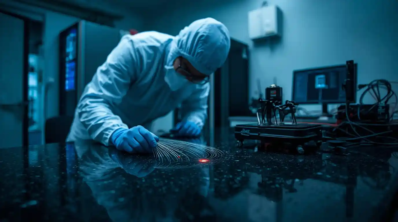
Silicon photonics alignment — the fiddly job of lining up a hair-thin optical fibre with a chip so the light actually goes in — has become one of the most expensive steps in modern chip making. An article published by AZoNano on 13 August 2026, reviewed by Andrea Salazar and built on work from motion-control maker PI (Physik Instrumente), argues the fix isn't a faster robot. It's a different order of operations.
Here's the money part. Industry and academic literature routinely puts packaging at more than 80% of what it costs to manufacture a photonic integrated circuit, and alignment is the biggest slice inside that. The die itself, printed thousands to a wafer, is the cheap bit. What burns cash is machine time spent hunting for the first flicker of light on every input and every output, one channel after another.
That matters here more than it used to. PsiQuantum is building a photonic quantum computer in Brisbane with close to A$940 million in combined federal and Queensland government backing, and photonic machines live or die on how many optical connections you can make cheaply and hold steady. Meanwhile market researcher MarketIntelo values co-packaged optics for AI data centres at about US$9 billion in 2025, heading toward US$122.5 billion by 2034.
Why Silicon Photonics Alignment Costs So Much
Light doesn't forgive sloppy positioning. Coupling a fibre to a waveguide needs nanoscale accuracy, and a real device usually has several inputs and several outputs that all need it at the same time. In the short waveguides typical of silicon photonics, the two ends interfere with each other — nudge the input to its peak and the output slides off its own.
The traditional answer was patience. Align the input, align the output, go back and redo the input, and keep looping until the whole device settles on a compromise everyone can live with. Each loop is machine time, and machine time is what turns a cheap die into an expensive finished product. Multiply by dozens of channels and the economics stop working.
How the Parallel Approach Actually Works
PI's pitch is a firmware-level system it calls Fast Multi-Channel Photonics Alignment, which pushes the search routines down into the controller instead of running them from a PC. Three things change.
Finding First Light Without a Blind Hunt
Rather than creeping across the chip looking for a signal, the controller runs a fast areal scan and fits a curve to the intensity it sees. On typical piezo nanopositioner setups with 100 micrometres of travel, that scan takes roughly 300 milliseconds. Finding first light has long been the slowest part of wafer probing and packaging, so shaving it pays off immediately.
Tuning Every Channel at the Same Time
Instead of sequential loops, the system optimises multiple channels, inputs, outputs and degrees of freedom concurrently and lands on a consensus position in one step. The interaction between the two ends stops being a problem to iterate around and becomes just another variable in the same calculation.
Holding It Steady While the Glue Cures
Alignment isn't finished when you hit peak power. Epoxy shrinks as it cures and parts drift with temperature, so the position you paid for can quietly walk away. Continuous tracking keeps nudging the stage during the cure, and because piezo actuators flex rather than slide, there's no mechanical wear from the constant correction.

From 60 Parts an Hour to a Few Hundred Milliseconds
This isn't new science suddenly appearing. Writing in Laser Focus World back in October 2017, PI's Scott Jordan and Stefan Vorndran noted that early-2000s photonics assembly ran at roughly 60 parts per hour per workstation, and that the term "photonomics" was coined in 2000 to push the industry toward automation. PI demonstrated parallel multi-axis alignment in 2015, and by 2017 was describing 18-axis systems.
Global consensus alignment (including tracking if desired) is achieved in one fast step.
The claimed payoff back then was two orders of magnitude — a hundredfold cut in alignment time. Worth remembering the source: these figures come from an equipment vendor and its sponsored technical articles, not an independent benchmark. The direction of travel is well supported, but treat the multiples as marketing arithmetic until a fab publishes its own throughput data.
What This Means for Australian Builders
Australia's photonics strength sits in research, sensing and specialist systems rather than volume packaging lines, so the near-term effect is on what local teams can buy and how fast overseas suppliers can deliver. Cheaper packaging widens what's affordable: LiDAR units for mining and agtech, fibre sensing for rail and pipelines, quantum hardware, and the optical interconnects inside every AI data centre being built along the east coast.
There's a sovereign-capability angle too. Every extra dollar of a photonic device that sits in packaging rather than in the wafer is a dollar spent on labour, tooling and skills that a country can, in principle, host itself. Assembly and test are far easier to stand up locally than a fab, and that's precisely the part of the cost stack this technology is squeezing.
What to Watch Next
If you're specifying photonics gear or writing a research grant this year, ask suppliers two blunt questions: does the alignment run in parallel across all channels, and does it keep tracking through the epoxy cure? Those two answers move quoted lead times and per-unit prices more than almost anything on the datasheet. Then watch the co-packaged optics ramp through 2027 — that's where the throughput claims get tested for real.




Comments 0